
Electronics & Schematics
This page is a guided tour of the PolyKybd Split72 electronics, sheet by sheet. The schematics below are the individual sheets of the KiCad project (Rev 3.2) — the same set bundled in the PDF documentation. Repeated per-key and buffer sheets are shown once, because every instance is identical.
The big picture
Section titled “The big picture”Each half is one 4-layer PCB carrying 36 identical key units, a shared RP2040 core, a shift-register block that expands a handful of MCU pins into the ~40 control lines the key array needs, a chain of non-inverting buffers that keep those signals clean as they cross the large board, and the power path (USB-C in, a 3.3 V regulator, and a separate display supply). The two halves are wired together over a USB-C link and talk to each other over a UART split connection; only the half plugged into the computer acts as the USB host side.
Board overview — left & right root sheets
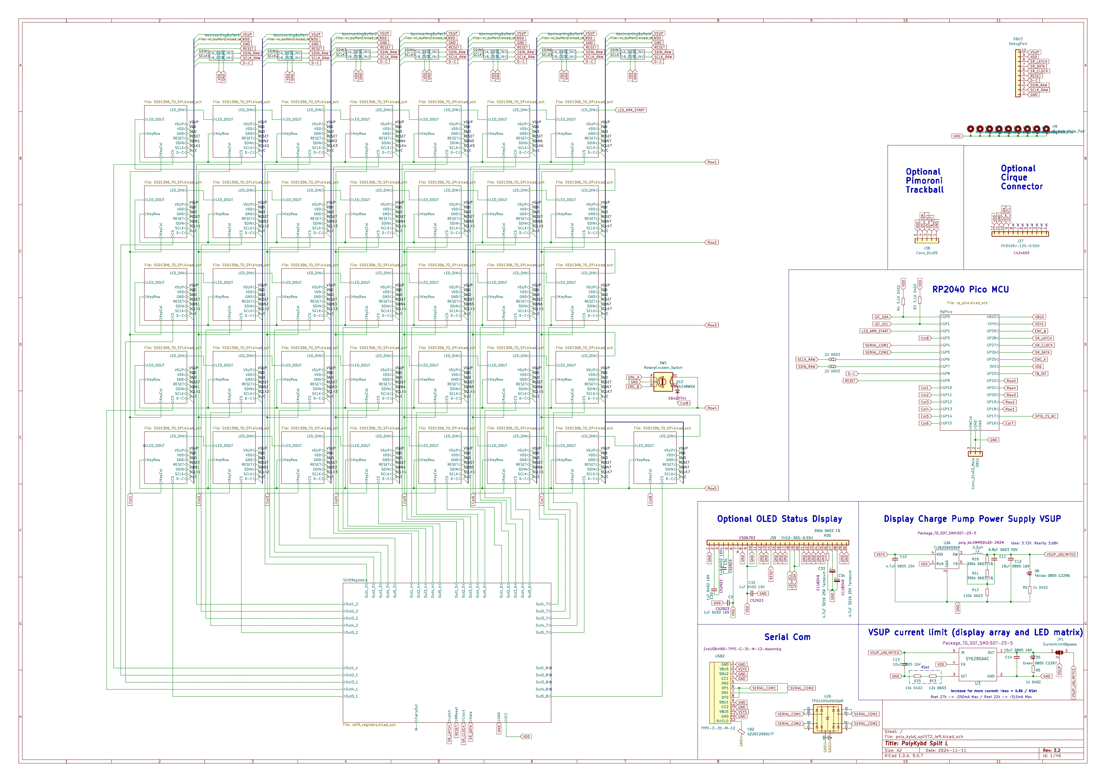
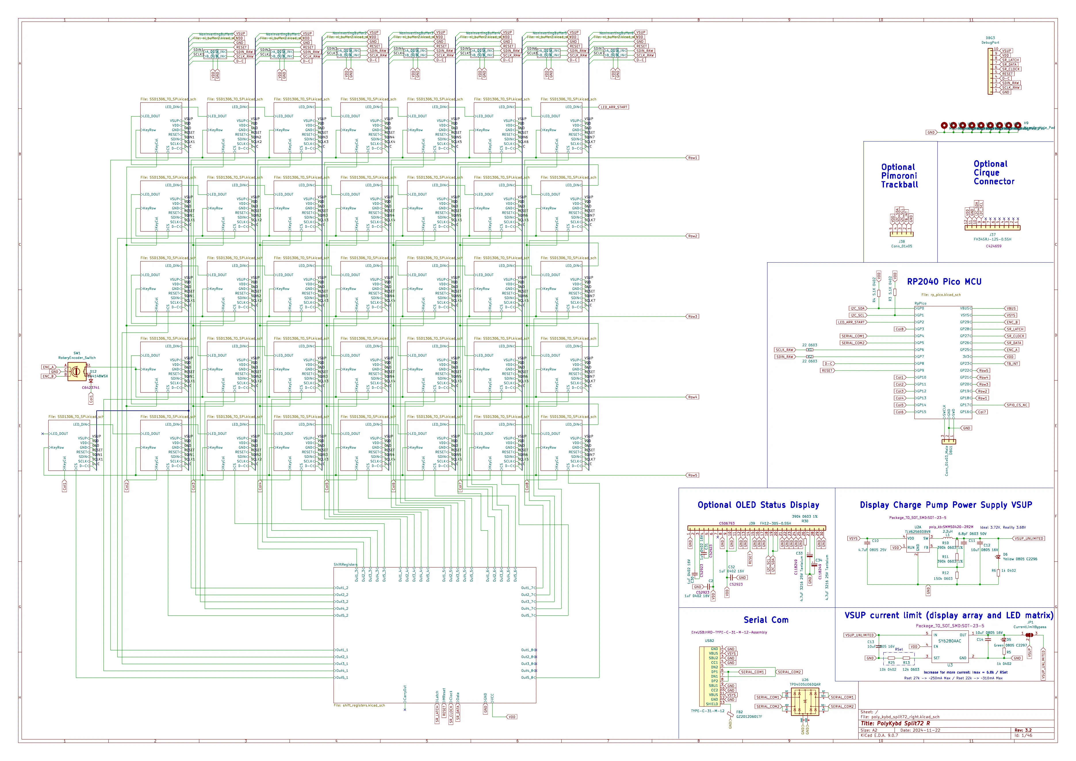
Section titled “Board overview — left & right root sheets”The top-level sheet of each board ties everything together: the 36 key units (each an instance of the Display Adapter, LED & Switch sub-sheet), the RP2040 block, the shift-register block, the display charge-pump supply (VSUP) with its current limiter, the USB-C link between the two halves, and the optional peripherals — the Pimoroni trackball / Cirque trackpad connector and the optional 0.96″ OLED status display.
Left half (“PolyKybd Split L”):
Right half (“PolyKybd Split72 R”) — structurally the same as the left, wiring up its own 36 key units, the shared control and power nets, and the non-inverting buffer blocks along the signal chain:
RP2040 — the microcontroller core
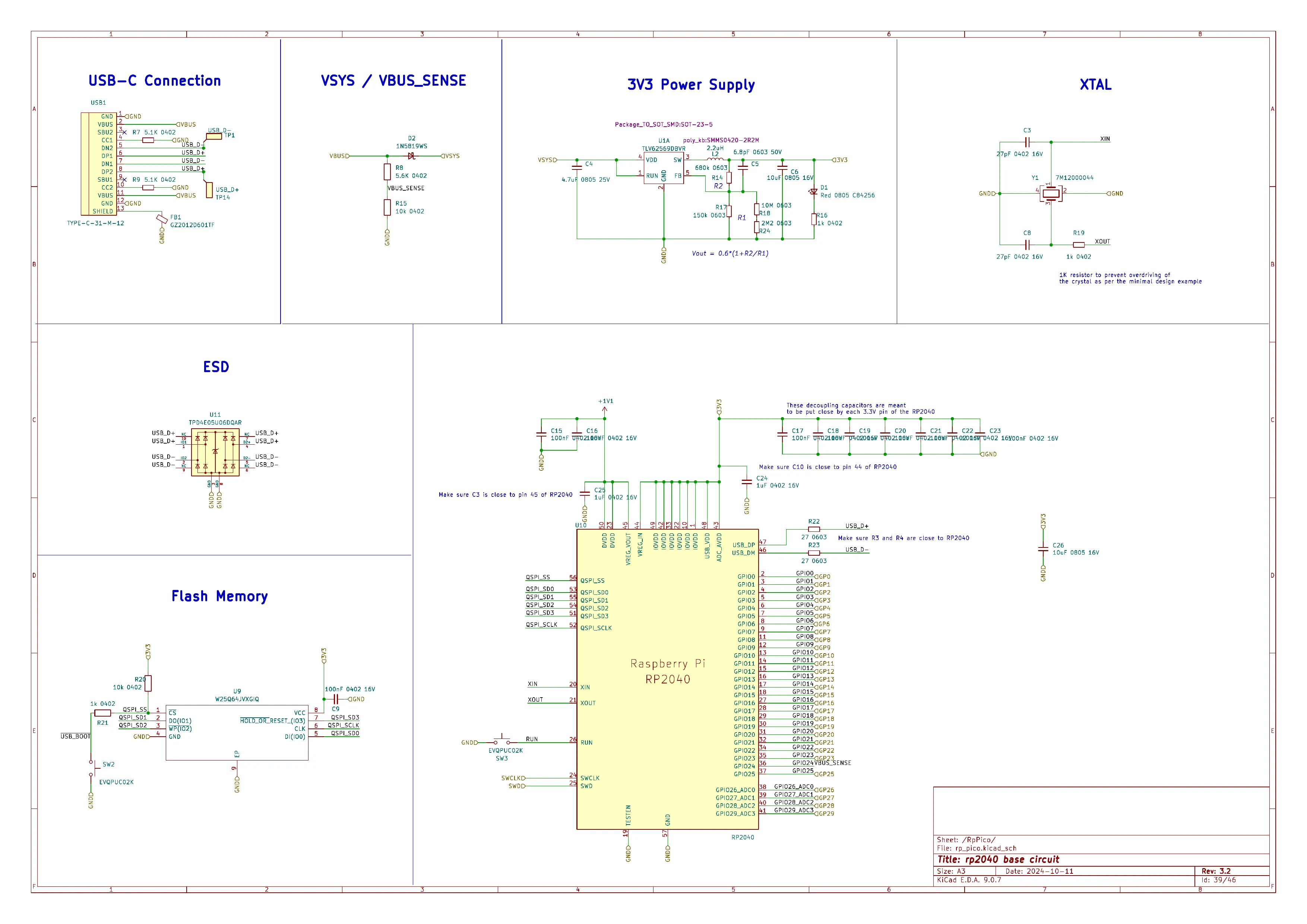
Section titled “RP2040 — the microcontroller core”The heart of the keyboard. This sheet contains the Raspberry Pi RP2040 (U10) with its decoupling network, the 8 MB QSPI flash (W25Q64, U9) and the BOOT button, the 12 MHz crystal (Y1), and the 3.3 V step-down regulator (TLV62569, U1) with its SMMS0420 inductor. It also holds the USB-C connector (USB1) with its ESD protection (TPD4E05, U11) and the VBUS-sense / VSYS network (including the 1N5819WS diode, D2) — so all of the power, USB, clock and boot circuitry lives on this one sheet.
Key block — one key unit (×36 per side)
Section titled “Key block — one key unit (×36 per side)”A single key unit, repeated 36 times per side. It contains the FH34SRJ FPC socket for the 0.42″ OLED display, the addressable RGB LED (XL-3030RGBC / WS2812B), the MX-compatible Kailh hot-swap switch with its 1N4148 matrix diode, and the local decoupling capacitors — i.e. the display, LED and switch of one key, all on one small repeated block.
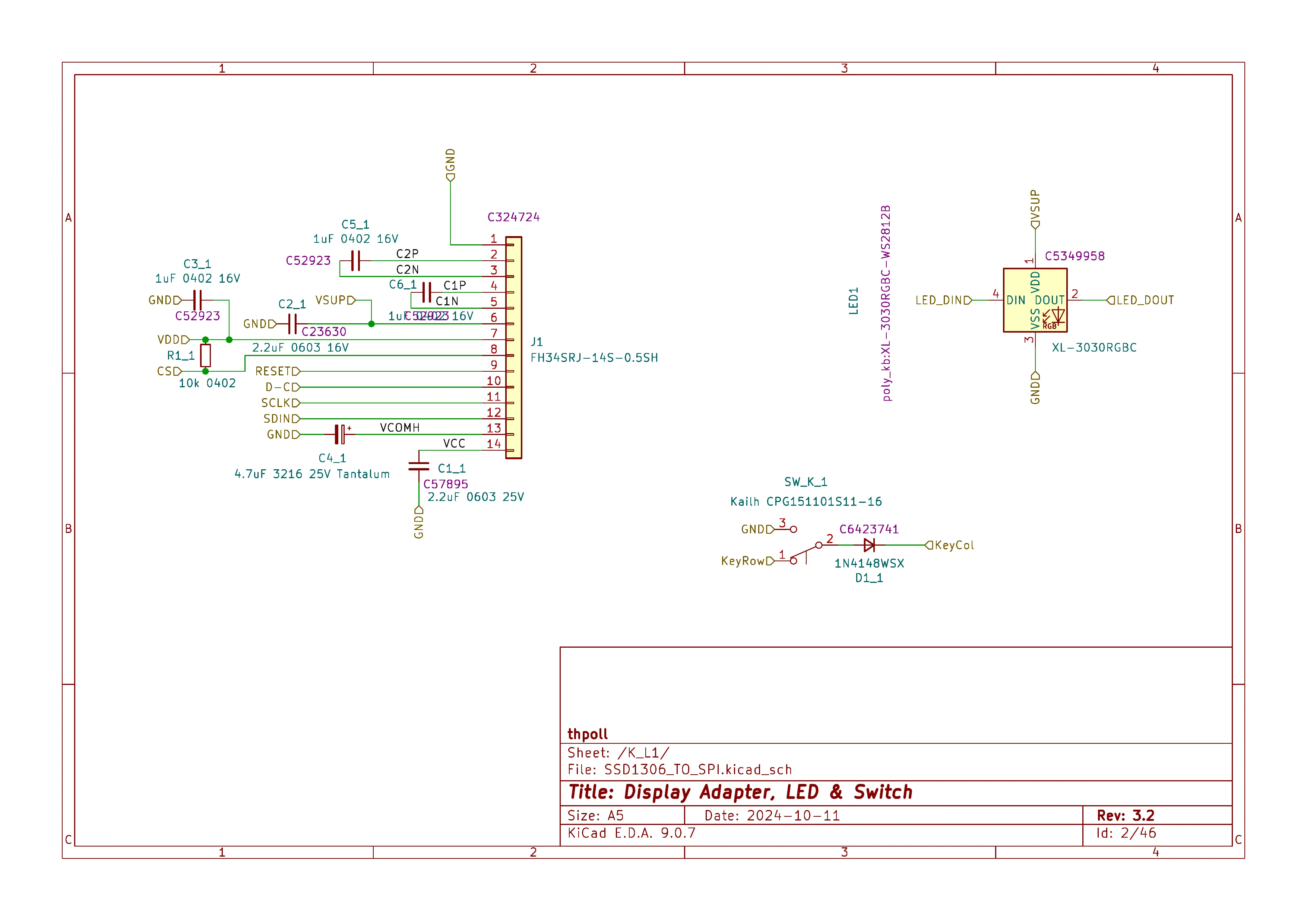
This is what makes every key independent: each has its own OLED to draw a legend on and its own RGB LED, addressed through the shift-register block below.
Shift registers — pin expansion
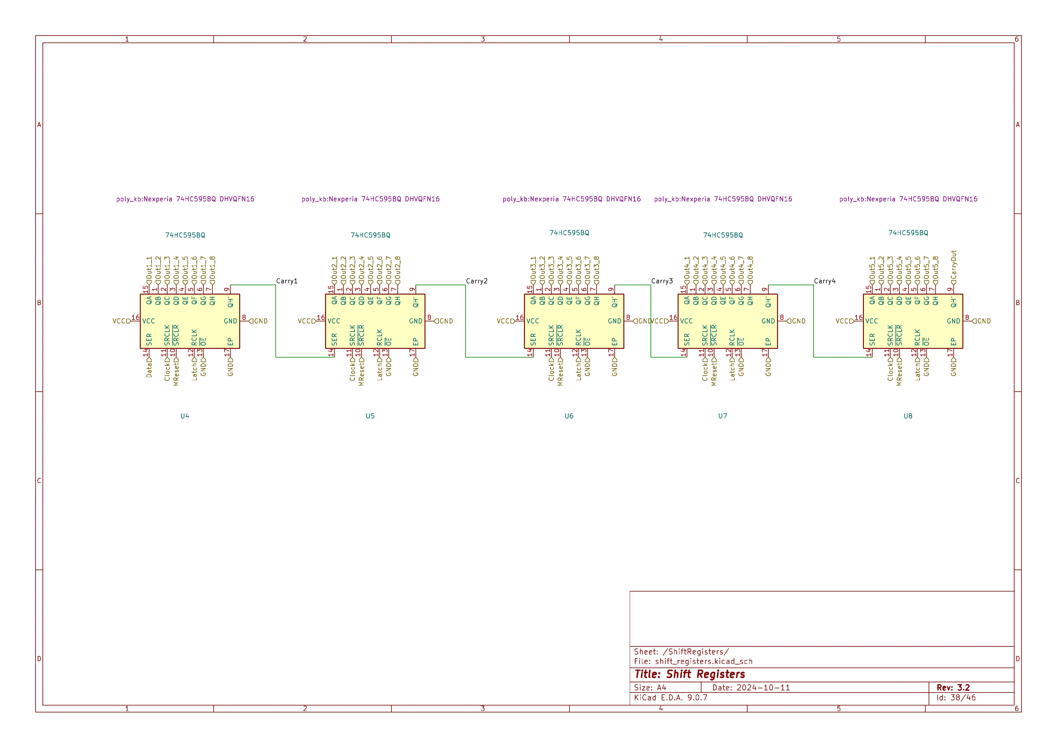
Section titled “Shift registers — pin expansion”Five 74HC595 8-bit shift registers (U4–U8) are daisy-chained together — each register’s QH'
output feeds the next one’s SER input via Carry1–Carry4 — and driven by the MCU’s Data /
Clock / Latch lines. They expand a handful of MCU pins into 40 control outputs used to address
the per-key hardware across the array.
Non-inverting buffers — clean signals across the array
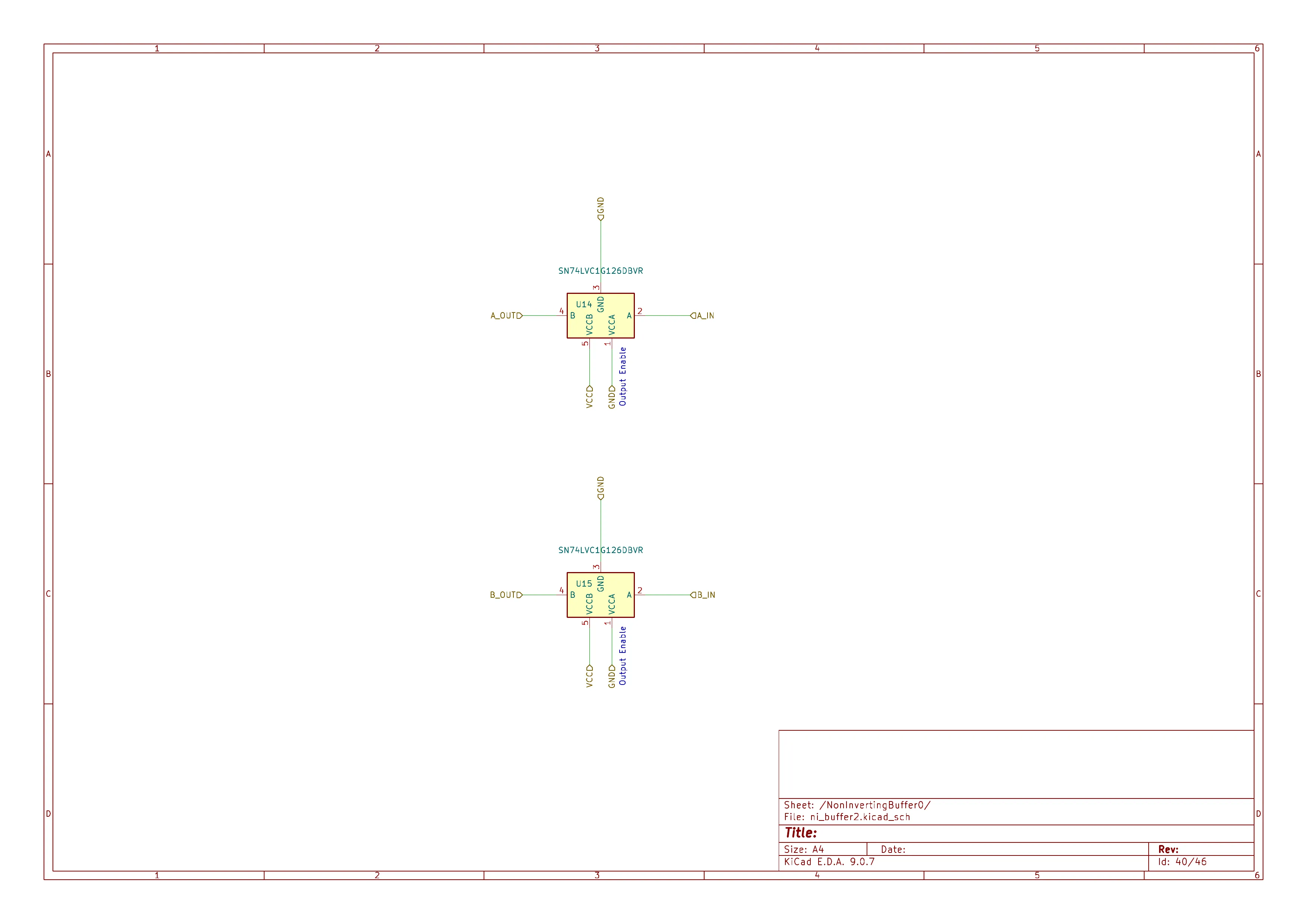
Section titled “Non-inverting buffers — clean signals across the array”A pair of SN74LVC1G126 single non-inverting buffers with 3-state outputs and separate A/B supply rails (U14, U15). This sheet is instantiated several times (NonInvertingBuffer0…5) to buffer and repeat the control/data signals as they travel across the large key array, keeping the signal edges clean over the distance.
Where to go next
Section titled “Where to go next”- PCB & Case Modification — the KiCad sources, gerbers, BOM and how to re-manufacture a modified board.
- PCB & Gerber Files — ordering the boards as-is.
- System Model & Data Flow — how the firmware drives all of the above.
- Displays & FPC Extension — the 0.42″ OLEDs that plug into each key unit.